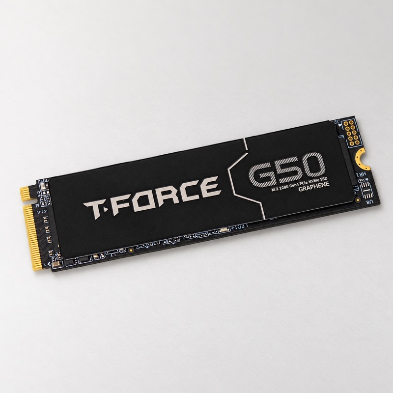
TEAMGROUP T-FORCE G50 1TB | Test Report
Test Platform
| Item | Test configuration |
|---|---|
| Drive | TEAMGROUP T-FORCE G50 1TB (TM8FFE001T); M.2 2280, PCIe Gen4 ×4 |
| Sample | One sample; serial number TPBF2503060040104304 |
| Firmware | 1.c.P.45 |
| Platform | NUC, Core Ultra 9 285H, 16 GB RAM; Ubuntu 26.04.1, Linux 7.0.0-38 |
| Tools | PyNVMe3 26.11; Quarch PPM for power measurement |
| PCIe Link | 16 GT/s ×4 |
| HMB | 128 MB |
Test Procedure
PyNVMe3 was used to test protocol, performance, power, stress, power cycling, and model reading.
| Category | Test ID | Scope |
|---|---|---|
| Protocol and reset | TP1 | Management, I/O, HMB, reset, power management, register and security functions; some tests were interrupted or skipped according to capability. |
| Low-power states | TP2.a | Power consumption and read/write response in low-power states. |
| Performance and power | TP2.b | Sequential, random and mixed I/O performance, response time and supply power at different write-workflow checkpoints. |
| Stress and data verification | TP2.c | A six-hour stress test ended after about 70 minutes due to a DSM command error; final full-drive verification was not performed. |
| Sudden power loss and recovery | TP2.d | 100 cycles planned; readiness timed out after power-on in the first cycle and recovery testing was not completed. |
| Normal power cycles | TP2.e | 100 cycles planned; readiness timed out after power-on in the first cycle and recovery testing was not completed. |
| Advertised performance | TP2.f | Peak sequential and random read/write performance in a small region. |
| Link speed switching | TP2.g | Fixed Gen5 and dynamic Gen2–Gen5 link-speed changes under a read workload. |
| Model loading | TP2.h | Read synthetic images of different sizes at various queue counts and queue depths. |
Product Radar
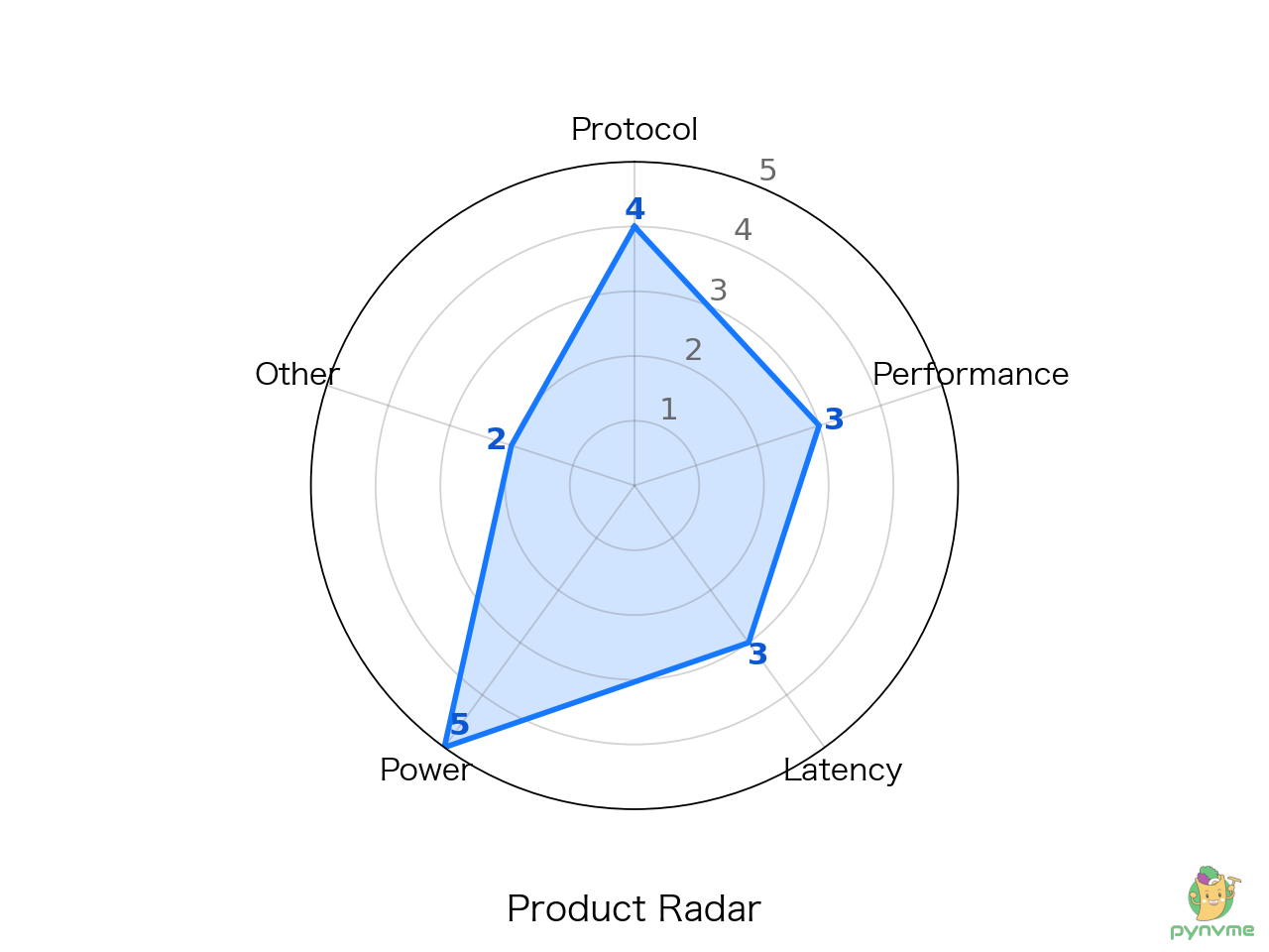
This chart shows five aspects of the tested sample. Protocol covers functions related to NVMe and PCIe specifications; performance covers read and write capability; latency concerns response time; power covers electricity consumption; and other includes stress, power cycling and recovery. Each dimension is scored from 1 to 5, with a higher score farther from the center. Protocol is scored 4: a command error ended the stress test early. Other is scored 2: the device remained inaccessible after queue testing, and normal and sudden-power-loss tests timed out waiting for readiness on the first cycle. The causes remain unknown.
Performance Positioning
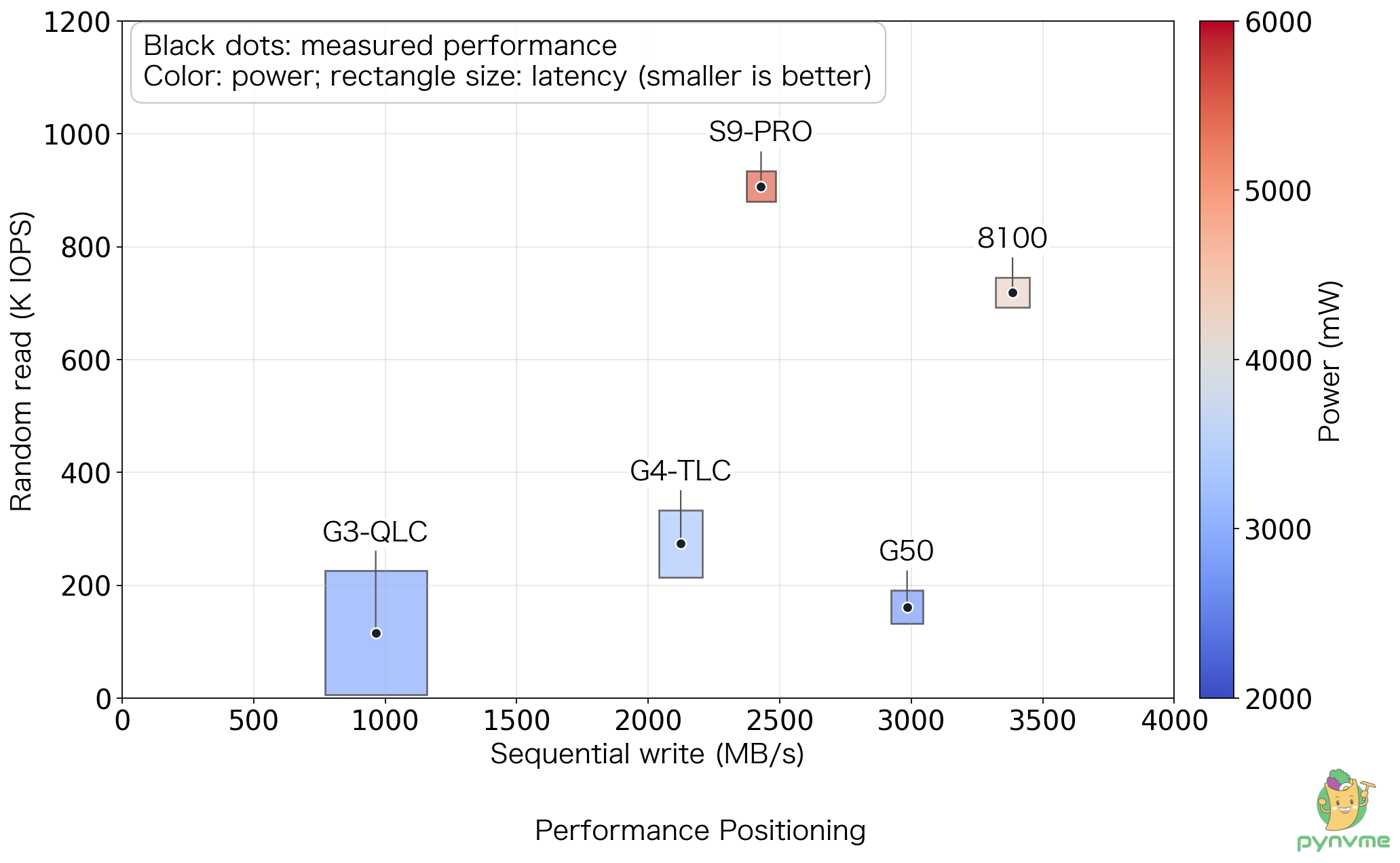
Each black dot places one drive according to two tests. Farther right means higher sequential write speed; higher up means stronger random read performance. The width and height of the rectangle represent longer response times in two workloads. Color represents power consumption during testing: blue is lower and red is higher.
Model Loading Time
This test simulates reading model images from an SSD and compares loading times at different queue counts and queue depths. G50 used a Gen4 ×4 link; G4 used Gen5 ×4.
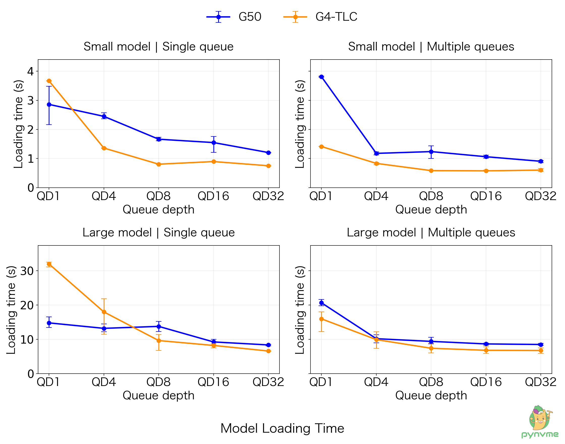
The four panels show small (4.7 GiB) and large (40 GiB) model images, each with a single queue and multiple queues. Queue depth on the horizontal axis is the number of read requests that each queue can issue at the same time; the vertical axis shows average read time. A lower line means the read completed sooner under those test conditions. Each point summarizes multiple measurements; the vertical bars show the observed range.
Key Issues
| ID | Test ID | Description |
|---|---|---|
| G50-01 | TP1.h | Queue deletion timed out during queue testing. The device then remained inaccessible and 35 subsequent initialization waits timed out; the cause is unknown. |
| G50-02 | TP2.d, TP2.e | Both normal and sudden power-cycle tests timed out waiting for readiness after the first power-on. Subsequent cycles were not completed and first-read recovery time could not be assessed. |
| G50-03 | TP2.c | A DSM command error ended the planned six-hour stress test after about 70 minutes; final full-drive verification was not performed. |
| G50-04 | TP1.b | Two power-loss readback tests with write cache disabled exited abnormally and did not produce complete results; the cause is unknown. |
| G50-05 | TP2.b | P99.9 latency during the full-drive write test was 401.111 ms; the longest response in the half-drive TRIM test was approximately 7.52 seconds. |
| G50-06 | TP2.h | Small-model loading time was longer than G4 under most queue conditions. |
| G50-07 | TP2.a, TP2.b | In low-power-state tests, first-read response was about 64 ms; the actual power state was not confirmed at each sampling point in the preset window. |